Application of HONSUN's Fiber Optic Plate & Fiber Optic Taper In CCD/CMOS
1. Application of HONSUN’s products in CCD/CMOS:
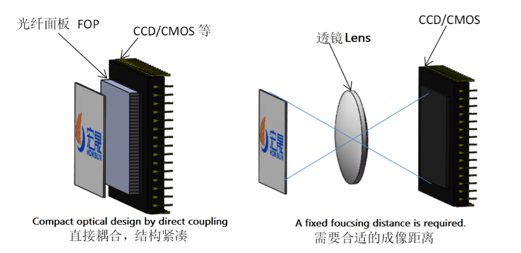
1) Fiber optic plate can be directly coulpled with CCD/CMOS to have compact optic design.
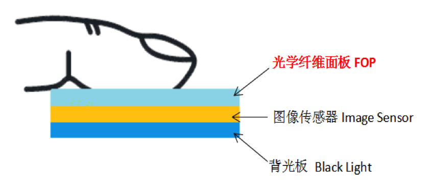
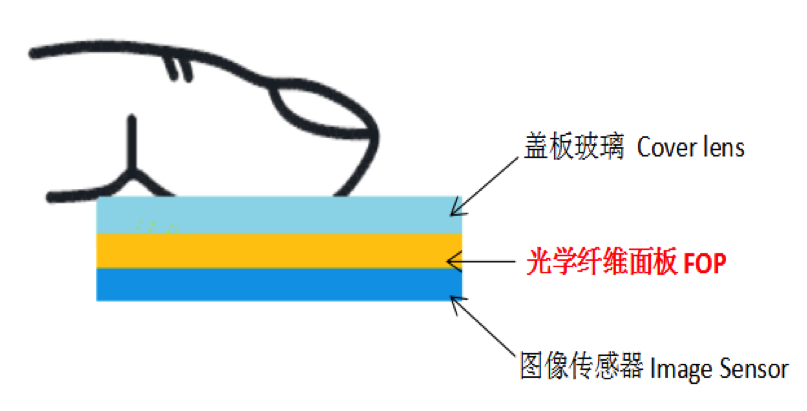
2) Fiber optic plate and fiber optic taper can be applied to the new-type fingerprint identification instrument as the imaging element with CCD.
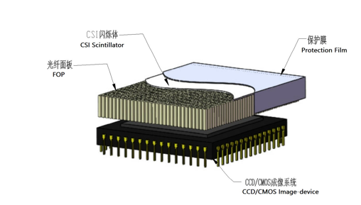
3) Fiber optic plate can be applied as X-ray Scintillator plate coupled with CCD/CMOS in DR dental X-ray imaging solution.
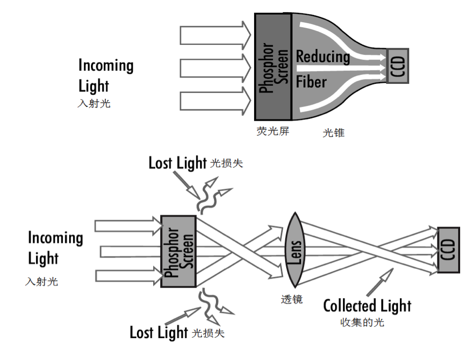
4) The small end of Fiber optic taper can be coupled with CCD/CMOS, which can be applied to the low-light-level camera tube.
5) The large end of FOT is plated with scintillator, and the small end coupled with CCD and applied to the imaging survey of invisible light and high-energy radiation such as x-ray camera, radiation imaging detector etc. FOT is also widely used in the field of medical treatment image technology and molecular biology, such as biological information study of small living animals, γ-ray camera, x-ray tomography, and Positron emission tomography Instrument.
2. What is CCD/CMOS sensor
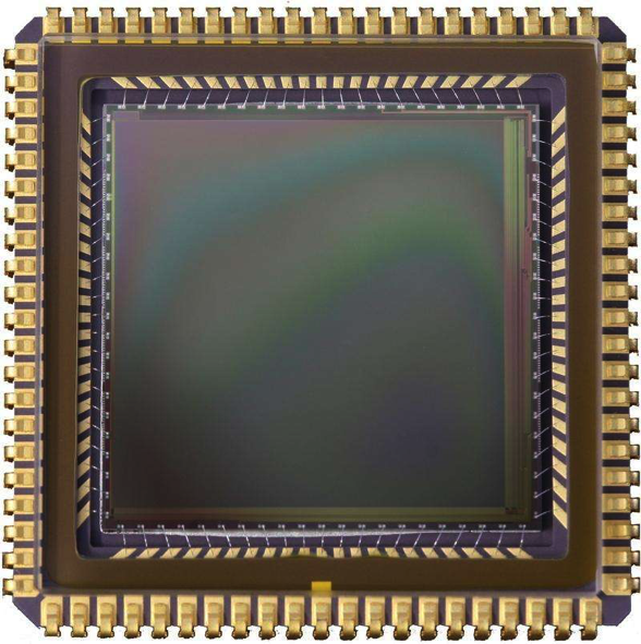
CMOS: CMOS, Complementary metal-oxide-semiconductor, is one of the logic families used in the manufacture of integrated circuits. An Active Pixel Sensor (APS) is a sensor able to detect light based on CMOS technology.
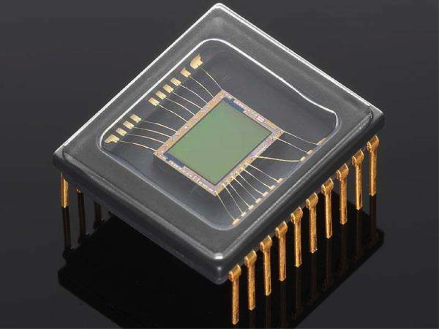
CCD: A charge-coupled device (CCD) is a device for the movement of electrical charge, usually from within the device to an area where the charge can be manipulated, for example conversion into a digital value. This is achieved by "shifting" the signals between stages within the device one at a time. CCDs move charge between capacitive bins in the device, with the shift allowing for the transfer of charge between bins.
3. What is the difference between CCD and CMOS
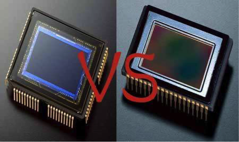
Digital cameras have become extremely common as the prices have come down. One of the drivers behind the falling prices has been the introduction of CMOS image sensors. CMOS sensors are much less expensive to manufacture than CCD sensors.
Both CCD (charge-coupled device) and CMOS (complementary metal-oxide semiconductor) image sensors start at the same point -- they have to convert light into electrons. If you have read the article How Solar Cells Work, you understand one technology that is used to perform the conversion. One simplified way to think about the sensor used in a digital camera (or camcorder) is to think of it as having a 2-D array of thousands or millions of tiny solar cells, each of which transforms the light from one small portion of the image into electrons. Both CCD and CMOS devices perform this task using a variety of technologies.
The next step is to read the value (accumulated charge) of each cell in the image. In a CCD device, the charge is actually transported across the chip and read at one corner of the array. An analog-to-digital converter turns each pixel's value into a digital value. In most CMOS devices, there are several transistors at each pixel that amplify and move the charge using more traditional wires. The CMOS approach is more flexible because each pixel can be read individually.
CCDs use a special manufacturing process to create the ability to transport charge across the chip without distortion. This process leads to very high-quality sensors in terms of fidelity and light sensitivity. CMOS chips, on the other hand, use traditional manufacturing processes to create the chip -- the same processes used to make most microprocessors. Because of the manufacturing differences, there have been some noticeable differences between CCD and CMOS sensors.
CCD sensors, as mentioned above, create high-quality, low-noise images. CMOS sensors, traditionally, are more susceptible to noise.
Because each pixel on a CMOS sensor has several transistors located next to it, the light sensitivity of a CMOS chip tends to be lower. Many of the photons hitting the chip hit the transistors instead of the photodiode.
CMOS traditionally consumes little power. Implementing a sensor in CMOS yields a low-power sensor.
CCDs use a process that consumes lots of power. CCDs consume as much as 100 times more power than an equivalent CMOS sensor.
CMOS chips can be fabricated on just about any standard silicon production line, so they tend to be extremely inexpensive compared to CCD sensors.
CCD sensors have been mass produced for a longer period of time, so they are more mature. They tend to have higher quality and more pixels.
Based on these differences, you can see that CCDs tend to be used in cameras that focus on high-quality images with lots of pixels and excellent light sensitivity. CMOS sensors traditionally have lower quality, lower resolution and lower sensitivity. CMOS sensors are just now improving to the point where they reach near parity with CCD devices in some applications. CMOS cameras are usually less expensive and have great battery life.
