HONSUN’s Fiber Optic Plate/Fiber Optic Taper Coupling To CCD and CMOS Image Sensors
Generally, X-ray semiconductor detectors employ two different detection schemes: direct and indirect. Direct exposure of the semiconductor devices with X-rays is limited to sensors with a large pixel size. For example, a single 10 keV X-ray photon will generate about 3000 electron-hole pairs which represent a significant amount of charge compared to a detector pixel well size of no more than about 60,000 electrons for high-resolution devices with pixel sizes of 10 um or less. Also, direct detection at X-rays energies beyond 10 keV quickly becomes highly inefficient: the silicon detector material is essentially transparent. A further complication arises from radiation damage to the unprotected semiconductor devices.
Hence, the indirect method of X-ray imaging using fluorescent screens optically coupled to semiconductor imagers addresses is the most popular method of X-ray imaging to date. Although the use of luminescent screens goes back to the early days of X-ray imaging, their development has seen major advancements over the last two decades with the creation of phosphors that produce visible light which is well matched to the sensitivity of silicon- based image sensors and with short decay times. Also, a range of materials is available with different densities suitable for a wide range in X-ray energies. To achieve a good sensitivity (high-luminescent light output) and a good spatial resolution, however, is still an area of active research.

In practice, guiding of the luminescent light to the sensor is performed using one of three methods: lens, reflective optics and fiber optics. Of these methods, the fiber optical (FO) methods provide the best efficiency of collecting the luminescent light and it is therefore not surprising that the majority of indirect detection schemes rely on this light coupling method. Typically, a manufacturer has a variety of different types of glass fiber (including strongly X-ray absorbing) combined with interstitial material (extra mural absorber EMA) with different levels of light absorption. For efficient coupling, the faceplates must be placed as close as possible to the sensor surface and fixed in position for reproducible imaging. Unfortunately, detailed procedures of how to couple (or mount) the fiber optics directly on image sensors have, to our knowledge, not been published of the commercially available solutions we have only found large pixel size frame-transfer charge coupled (CCD) sensors for which a typical bond layer thickness was quoted to be 20 μm. This bonding layer thickness was simply too large for our application.
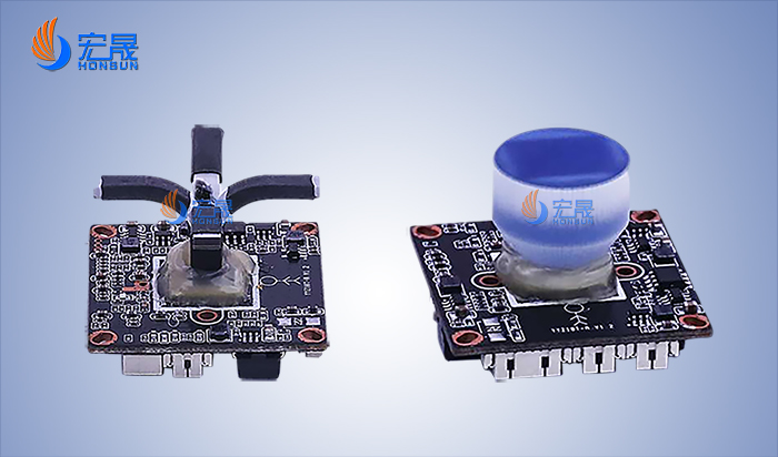
HONSUN customizes fiber optic plate and fiber optic taper according to customers’ requirements no matter in qualifications or dimensions. We have fiber optic plate and fiber optic taper applicable for X-ray detection, with high resolution and high contrast. The glass materials provide inert and durable surface properties, for compatibility with optical coatings and bonding materials
